Is Huawei already on the waiting list?
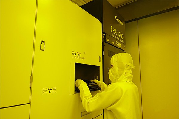
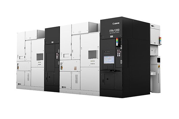
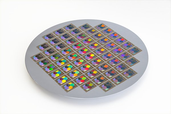
Canon introduced a setup called FPA-1200NZ2C, which allows the production of 5-nanometer chips. This is the first commercial solution of its kind, but there will be others: Canon will develop the system in the future so that it can be used to produce 2-nanometer chips.

The most important thing is that it uses an alternative approach to conventional photolithography. The FPA-1200NZ2C is based on the principle of nanoimprint lithography: instead of a photomask as in classical optical lithography, a stamp with a nanorelief is used. The nano relief, in turn, serves to form a mask from a polymer layer on the surface of the semiconductor substrate. Canon claims that nanoimprint lithography is simpler and cheaper.

Canon has unveiled a commercial setup that allows it to “print” 5nm chips without photolithography
“ Because the new solution does not require a special wavelength light source, it can significantly reduce power consumption compared to state-of-the-art semiconductor photolithography equipment, thereby helping to reduce CO2 emissions, ” Canon said.

It is unlikely that the equipment of the Japanese company will be of interest to the same TSMC, but, for example, in China, they would be happy to get machines that can produce 5-nanometer chips. Huawei has already increased its purchase volumes of ASML DUV lithographs, and it is possible that it will also be interested in the FPA-1200NZ2C.


