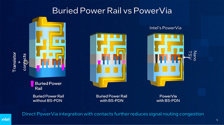
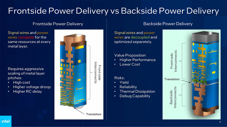
It allows transistors to consume electricity from one side of the chip, using the other side to connect to data links.
Intel boasted that it had developed and already tested the world’s first solution for powering chips from the back. More specifically, PowerVia technology allows transistors to draw power from one side of a chip while using the other side to connect to data lines.
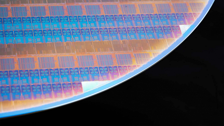
Intel’s new development solves interconnect bottlenecks for area scaling by moving power routing to the back of the wafer.
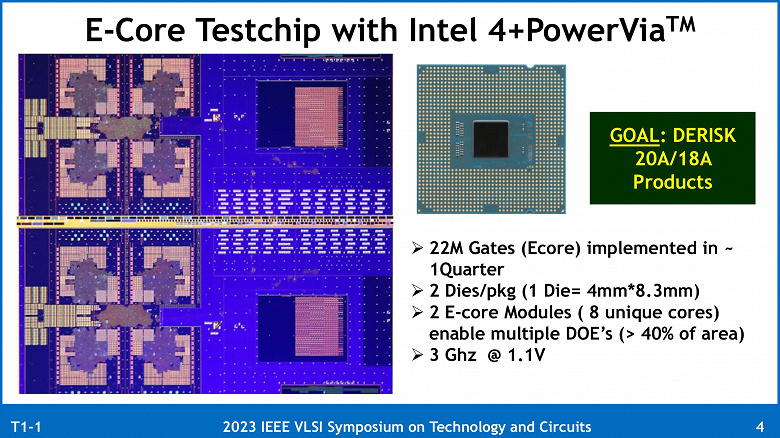
PowerVia is an important milestone in our aggressive five-node-in-four-year strategy and on our journey to reach a trillion transistors per package by 2030. Using the trial technology node allowed us to reduce the risk associated with backup power for our leading technology nodes, placing Intel one node ahead of the competition in bringing reverse power to the market.
Intel has unveiled a weapon against TSMC and Samsung.
PowerVia technology is slated for commercial deployment as part of the Intel 20A process as early as next year. And according to the description, one would think that for consumers it still does not matter, but this is not so. The bottom line is that this technological solution allows chip developers to make their products more productive. In particular, Intel itself managed to achieve a performance increase of 6% on a Meteor Lake test processor with small cores. In addition, PowerVia has reduced work stress by more than 30%.
Thus, this technology can allow Intel to create both its own more competitive processors and offer its capacity to other companies as part of Intel Foundry Services.
The company has previously said that PowerVia will be one of two technologies that will allow Intel to overtake TSMC and Samsung.


